Yale University’s Center for Research on Interface Structures and Phenomena (CRISP) is one of the National Science Foundation (NSF)-funded Materials Research Science and Engineering Centers (MRSECs) and is part of NSF’s Center of Excellence for Materials Research and Innovation (CEMRI). The CRISP MRSEC is a partnership of Yale University and Southern Connecticut State University.
Dr. Sohrab Ismail-Beigi and his research group at CRISP are working to create new materials with useful electronic properties by taking existing materials and modifying their structure at the level of the bonds between the constituent atoms. This is feasible because the distribution of electrons around an atom is sensitive to subtle atomic-scale distortion of its bonds.
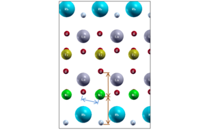
Using modern theoretical methods, the team have discovered a new materials design principle applicable to a broad class of layered materials that allows one to selectively elongate bonds. The example above shows how the bonds that a nickel atoms makes can be elongated in the vertical direction (orange) compared to the horizontal direction (blue). In this case, an oxidized nickel layer (green Ni, red O) has an oxidized titanium layer (yellow Ti) above it and all are surrounded by insulating oxidized layers of Lanthanum (grey La) or the insulator rubidium fluoride (blue Rb and small grey F).
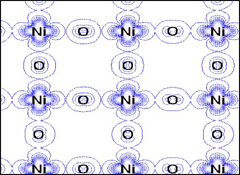
One consequence of such elongation is that the atomic orbitals of the nickel atom become inequivalent. Here, the conducting electrons in the system reside on the nickel atoms and only inhabit atomic orbitals of a particular shape that line in the nickel-oxygen plane. Below we see the spatial distribution of conducting electrons in that plane showing how they can meander among the nickel and oxygen atoms in the plane.
This type of planar electronic distribution also occurs in high-temperature superconductors, and these materials design principles may aid in potentially finding new materials with high temperature superconductivity.